Thick Film Printing
Thick-film printing uses conductive, resistive and insulating pastes, deposited in substrate by screen printing technology (silk screening). For different markets served, substrate can divided into AIN, Al2O3, Enamel, Sapphire, Glass, Stainless steel, etc. So far, the ceramic substrate is the most commonly used substrate material in Thick-Film hybrid IC industry.
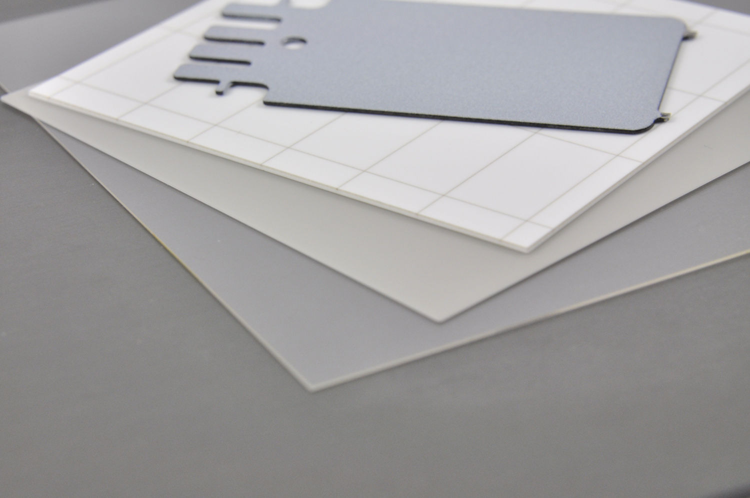
Substrates materials
- Main substrate: Al2O3 (16, 25, 32, 40mil)
- Others: AIN, Enamel, Sapphire, FPC, Glass, Silicon Chip, Stainless steel, etc.
- Maximum Size: 6 inches by 6 inches (<6”x6”)
Printing Capabilities
- Double side and Through hole printing
- Multilayer printing: 2~7 layers
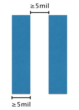
- Minimum line widths: 5 mil
- Minimum line space: 5 mil
- Precise thick film resistors : Customer circuit design

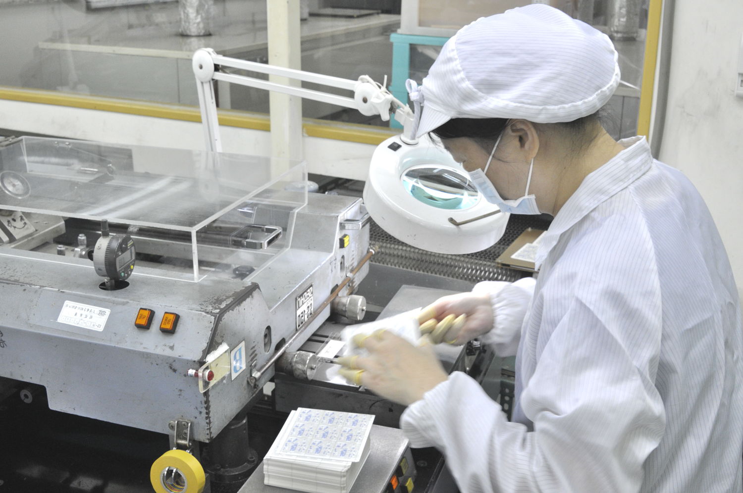
Total Quality Control
- 100% Stereo Microscope + Visual Inspection
- Inspection tools includes Metroimage 2.5D, In circuit test (ICT), Magnify Lamp10X, Micrometer Caliper